| Session Time | Name, Affiliation, Paper Title and Short Biography |
|---|---|
| 27A-2-1 13:30 | Prof. Takahiro Kozawa, Osaka Univ., Japan EUVL Stochastics Symposium 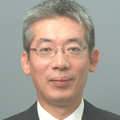 Takahiro Kozawa is a professor of the Institute of Scientific and Industrial Research (ISIR), Osaka University. He earned his BS and MS degrees in nuclear engineering from the University of Tokyo, and Ph. D. degree in chemical engineering from Osaka University in 1990, 1992, and 2003, respectively. His work is mainly focused on beam-material interaction and beam-induced reactions in resist materials. |
| 27A-2-2 13:45 | Mr. Kazuishi Tanno, Tokyo Ohka Kogyo, Japan Development status of EUV Chemically Amplified Resist 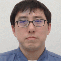 He has been with over 13years R&D experience in advanced lithography material since joined Tokyo Ohka Kogyo Co., Ltd (TOK) in 2008. He has been engaged in development work related to the resist material and process on ArF lithography, then currently he`s working on EUV lithography development. |
| 27A-2-3 14:15 | Dr. Toru Fujimori, FUJIFILM Corporation, Japan The status of stochastic issues - Photon stochastic and Chemical stochastic -  TORU FUJIMORI, is Manager of FUJIFILM Corporation to manage for photo resist development group. He received B.S. and M.S. degrees in organic chemistry from Saitama University, Japan, in 1989 and 1991, respectively. In 1991, he joined FUJIFILM Corporation as a researcher in synthetic organic chemistry laboratories. He has been studying for synthesizing new materials for photo films for 3 years, and then for semiconductor materials (photo resist materials) for 8 years. In 2002, He has moved to electronic materials research laboratories to study color resist for image sensor for 6 years. Since 2008, he has been studying photo resist materials for KrF, ArF, ArF immersion, EB and EUV lithography as a research manager. From 2014 to 2016, he was senior researcher at EIDEC (EUVL Infrastructure Development Center, Inc.) as an assignee from FUJIFILM. He has filed over 200 patents in this field, described a lot of papers, presentations and chapter of the photo resist text book. |
| 27A-2-4 14:45 | Mr. Hirokazu Matsumoto, ZEON, Japan The study of chain scission type photo resist for EUV lithography  Hirokazu Matsumoto is the General Manager of Specialty Chemical Lab, ZEON CORPTATION. He is leading the material development in the Electronics field, including dry etching gas, insulation materials, photo resist, EB resist, and EUV resist. |
| 27A-3-1 15:45 | Prof. Yusa Muroya, Osaka University, Japan Study on beam-induced transient reaction process of carboxylic acids used as ligands of metal oxide nanocluster resists 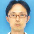 Yusa Muroya was received Ph.D degrees in engineering from Univ. of Tokyo, Japan, in 2007, and is now working at Institute of Scientific and Industrial Research, Osaka University, Japan. His research interest includes fundamental and application study of quantum beam-induced physical chemistry and chemistry of condensed inorganic/organic matters relating to nuclear engineering and next generation lithography, such as subcritical- and supercritical- fluids, solutions containing complex and nanoparticles. Applying various beam sources such as an electron linear accelerator and a femtosecond laser, he is advancing to elucidate key roles of short-lived transient intermediates played for the functional expressions. |
| 27A-3-3 16:15 | Prof. Takeo Watanabe, University of Hyogo, Japan Fundamental Study of the Origin of the Stochastics in EUV Resist 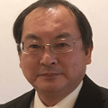 Takeo Watanabe received his Ph.D. from Osaka City University in 1990. He is Full Professor, Director of Center for EUV, and Dean Laboratory of Advanced Science and Technology for Industry, University of Hyogo. He is an expert of the EUV lithographic technology, including optics, exposure tool, mask and resist related technologies. He has authored over 200 technical papers, and he is international affairs, and the organizing and program committee members, of the International Conference of Photopolymer Science and Technology (ICPST). He is also Conference Chair of the International Conference of Photomask Japan. And he is a program committee member of EIPBN. |
| 27A-3-4 16:45 | Prof. Mark Neisser, Tan Kah Kee Innovation Laboratory, China The Lithography Roadmap and the Impact of Stochastics  Mark Neisser is Technology Director for the Industrialization Platform at the Tan Kah Kee Innovation laboratory at Xiamen University in Xiamen, China. He is also adjunct professor in the College of Semiconductor Science and Technology at Xiamen University. He has worked in the semiconductor industry for over thirty years including managing R&D at IBM, AZ Electronic Materials and SEMATECH. He received his B.S. degree in chemistry from the Cornell University and his M.S. and Ph.D. degrees from the University of Michigan. He is the author of more than 30 patents, over 100 journal papers and has co-authored two book chapters. He is the chairman of the IRDS roadmap lithography committee. |
| 27A-4-1 18:30 | Mr. Eelco van Setten, ASML, Netherlands High-NA EUV Imaging and stochastics: From system introduction towards low-k1 extension  Eelco van Setten received his MSc in Applied Physics from the University of Twente in the Netherlands in 1999 and joined ASML in 2000. He has worked on the evaluation and understanding of the imaging performance of ASML’s scanners for many generations and technology nodes, covering KrF, ArF, immersion and EUV. Currently he is working as System Engineer for EUV imaging on the development of ASML’s high NA EUV lithography tool. |
| 27A-4-2 19:00 | Dr. Danilo De Simone, Imec, Belgium Materials for Extreme Ultraviolet Lithography: State of the Art and Challenges towards High-NA  Danilo De Simone has 21 years of experience in R&D semiconductor in the field of nanolithography and patterning materials. He has been working in the industry for STMicroelectronics, Numonyx and Micron Technology. In 2013, he joined the international nanoelectronics research center IMEC in Belgium as principal staff member leading the research on patterning materials for EUV lithography. |
| 27A-4-3 19:30 | Dr. Yasin Ekinci, Paul Scherrer Institute, Switzerland Stochastic challenges for the ultimate resolution in photolithography  Yasin Ekinci is head of the Laboratory of Micro and Nanotechnology at Paul Scherrer Institute, Switzerland. He obtained his PhD in Max-Planck Institute for Dynamics and Self-Organization, Göttingen, Germany in 2003. In 2004, he joined Paul Scherrer Institute as a postdoctoral researcher. Between 2006 and 2012 he worked as a postdoctoral researcher and subsequently as a senior scientist and a lecturer in Department of Materials at ETH Zürich. He is at PSI since 2009 working on various topics of nanoscience and technology, including EUV lithography, resist materials, lensless imaging, plasmonics, semiconductor nanostructures, and nanofluidics. He is author/co-author of more than 220 papers and 7 patent applications. He is a fellow of SPIE. |
| 28A-1-1 9:00 | Dr. Anna Lio, Intel, USA Traversing from 0.33 NA to 0.55 NA EUV lithography: a EUV resist perspective  Dr. Anna Lio is a Senior Principal Engineer at Intel Corporation, Portland Technology Development. She manages the development of all EUV lithography materials for Intel’s current and next generation technologies. She joined Intel in 1997 and has worked in the area of photoresist and photolithography, design rules definition, microprocessor process development and integration for every Intel’s technology starting at the 130nm node. She received 3 Intel Achievement Awards, Intel’s highest technical recognition and became an SPIE Fellow in 2021. Anna holds a M.S. in Physics from the University of Pisa (Italy) and a PhD in Electrical Engineering from the University of Glasgow (UK). |
| 28A-1-2 9:30 | Mr. Toshiyuki Hisamura, Xilinx, USA Optimization of EUV process for 7nm Versal production  Toshiyuki (Toshi) Hisamura is Principal Engineer and Senior Manager of Xilinx, Inc. (USA) who has been managing lithography and mask technology development group since he joined the company in 2000. Prior to that, he held a variety roles involving international business development at Toppan Printing. Hisamura holds two U.S. patents (one pending). He earned a bachelor's degree from Waseda University in 1987. |
| 28A-1-3 10:00 | Dr. Azat Latypov, Siemens Digital Industries Software, Inc Fast quantification of EUV stochastic defect probabilities using Gaussian Random Field models  Azat Latypov is a Senior Member of Technical Staff at Siemens Digital Industries Software, Inc, Siemens EDA (formerly Mentor Graphics Corporation), leading the development of novel fast EUV stochastic models for the full-chip OPC and verification. Prior to joining Siemens, Dr.Latypov worked on computational algorithms and simulations in US semiconductor industry (GLOBALFOUNDRIES, KLA, ASML, IPEC Precision) with applications to directed self-assembly (DSA), optical photomask inspection, optical maskless lithography, plasma wafer planarization/shaping and wafer metrology. Dr.Latypov holds 27 US patent families (over 40 US patents), multiple Asian and European patents, and he authored or co-authored a book chapter and 35 papers in refereed journals and conference proceedings. Azat Latypov earned his Ph.D. in Applied Mathematics from University of Windsor, Canada and a MSc degree from Moscow Institute of Physics and Technology, Russia. |
| 28A-2-1 11:00 | Dr. Lawrence Melvin, Synopsys, USA Applying Stochastic Simulation to Study Defect Formation in EUV Photoresists  |
| 28A-2-2 11:30 | Dr. Rajan Beera, Pall, USA Defect Reduction in EUV Lithography Materials using High Performance Filtration  Rajan Beera is the Chief Technology Officer at Pall Industrial, a Danaher operating company. Prior to the current role, as the Vice President of Global R&D for Pall Microelectronics, he led the research & development of advanced filtration, separation & purification products for semiconductor process applications. Dr. Beera started his career in the Semiconductor Industry as a process engineer in photolithography and held various technology leadership roles of increasing responsibility at National Semiconductor and Texas Instruments. He received his Ph.D. in Electrical Engineering from University of Arkansas (USA). |
| 28A-2-3 12:00 | Dr. David Medeiros, Entegris, USA Addressing the Defectivity Challenges of EUV Lithography  David Medeiros joined Entegris as a Senior Director of Engineering in the office of the CTO in April of 2021. Previously he spent six years at GLOBALFOUNDRIES, first as the Senior Director of Patterning at Fab 8, and later as the Vice President of Global Engineering. Prior to GF, he spent seventeen years at IBM, culminating as the Director of Patterning R&D. His career began in the semiconductor industry as a synthetic chemist at Shipley Company. David holds a PhD in Chemistry from the University of Texas, Austin and a BS in Chemistry from the University of Massachusetts, Amherst. |
| 28A-3-1 13:30 | Dr. Hakaru Mizoguchi, Gigaphoton, Japan Update of >300W High Power LPP-EUV Source Challenge IV for Semiconductor HVM 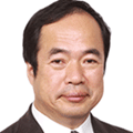 Hakaru Mizoguchi is Senior Fellow of Gigaphoton Inc. and Guest Professor of Kyushu University in Japan (2021-). He is Fellow of The International Society of Optical Engineering (SPIE, 2019-), and member of The Laser Society of Japan and The Japan Society of Applied Physics. He received a diplomat degree in plasma diagnostics field from the Kyushu university, Fukuoka, Japan in 1982 and join Komatsu ltd.. He joined CO2 laser development program in Komatsu. After that he was guest scientist of Max-Plank Institute Bio-Physikalish-Chemie in Goettingen in Germany 2 years 1989-1990. Since 1990 he concentrated on KrF, ArF excimer laser and F2 laser research and development for lithography application. He got Dr. degree in high power excimer laser field from Kyushu university in 1994. In 2000 Gigaphoton Inc. was founded, since then he was one of the founders of Gigaphoton Inc.. From 2002 to 2010 he organized EUV research group in EUVA program, since then he has been promoting EUV light source product development up to now. He got Sakurai award from OITDA Japan in 2018. Also he got IAAM Scientist Award in Advanced Materials Lecture Series in 2020. |
| 28A-3-2 14:00 | Dr. Seiji Nagahara, Tokyo Electron, Japan EUV resist material and process optimization for reducing stochastics effects in EUV lithography 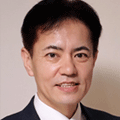 Seiji Nagahara is Principal and Chief Scientist in Tokyo Electron Ltd (TEL). He now works for marketing and development of the next generation coater and developer equipment and technologies for future lithography in TEL. Prior to joining TEL, he was a lithographer in Renesas Electronics, NEC Electronics, and NEC. He researched lithography related technologies in a variety of places including IMEC (Belgium), University of California, Berkeley (USA), Argonne National Laboratory (USA), EIDEC (Japan) and Toshiba (Japan) in addition to TEL. He took Bachelor, Master, and Ph.D. degrees in Engineering at Osaka University, Japan. He is active as an author of technical papers, book chapters, and patents in patterning technologies. He also contributes to the academic and technical societies as a committee member including Program Committee Chair of MNC2021. |
| 28A-3-3 14:30 | Mr. Yasutaka Morikawa, Dai Nippon Printing, Japan A study of the effect of EUV masks on the EUVL stochastics 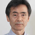 Yasutaka Morikawa is Engineering Manager of Dai Nippon Printing Co., Ltd. (DNP) to lead EUV mask development. He has 25 years of experience in Photomask’s R&D for semiconductors from KrF to EUV. He has been involved in the development of many kinds of Phase Shifting Masks and also NIL Templates. He is the author/co-author of over 70 technical papers and several book chapters. He received B.S. degree in Chemical Engineering from Tokushima University in 1986. |


