| Section | Invited Speaker's Name and Affiliation | Paper Title | Short Biography |
|---|---|---|---|
| 1-1: Advanced Lithography and Patterning 29A-3-1 13:30, October 29 | Fukasawa Ikuya HOYA, Japan  | Challenge of attenuated phase shift mask for EUV lithography | Ikuya Fukasawa joined HOYA Corporation in 2019. He is an engineer related to film coating in the Blank Division and working for the development of EUV mask blank. He received the Best Paper Award about EUV attenuated phase shift mask at the 27th symposium on photomask and NGL mask technology, Photomask Japan 2021. |
| 1-2: Electron and Ion Beam Technologies 29A-4-1 15:30, October 29 | Sun Wei, Hitachi, Japan | Deep learning model for 3D profiling of high-aspect-ratio features using high-voltage CD-SEM | |
| 1-3: Patterning Materials 29A-2-1 11:00, October 29 | Prof. Dong Ki Yoon, KAIST, Korea | Light-driven fabrication of helical nanostructures and their optical applications | Dong Ki Yoon received his Ph.D. degree in chemical and biomolecular engineering from KAIST in 2007. After working on the next-generation nanofabrication project in Samsung Electronics for two years, he joined the department of physics at the University of Colorado, Boulder, for his postdoctoral research and focused on the study of the novel phenomena of liquid crystals in marginal space. Following this, he joined KAIST in 2011. Currently, he is a full professor in the Department of Chemistry, leading the ‘Soft Material Assembly group’ to pioneer the patterning and display applications based on soft materials such as liquid crystals, supramolecules, biomaterials and polymers |
| 2-1 Nanocarbon & 2D Materials 28B-1-1 9:00, October 28 | Prof. Iwao Matsuda, Univ. of Tokyo, Japan | Evolutions of the Dirac Fermions in Monatomic Layers | 2001.3 Ph-D degree (Science) (School of Science, the University of Tokyo, Japan) 2001.4-2001.8 JSPS postdoc fellowship (Department of Physics, the University of Zuerich, Switzerland) 2001.9-2006.11 Research Associate (Department of Physics, the University of Tokyo, Japan) 2006.12-2021.3 Associate Professor (Institute for Solid State Physics, the University of Tokyo) 2021.4-present Professor (Institute for Solid State Physics, the University of Tokyo) Current Research Interest: -Synthesis and growth of novel monatomic layers -New techniques of systems of operando spectroscopies using synchrotron radiation, X-ray free-electron laser and high-harmonic generation lasers -Dynamics of carriers, spins, and molecules at surfaces and monatomic layers Research Achievements: -Measurement of resistance at a surface monatomic step by four-tip STM -Experimental proof of the topological insulator by high-resolution spin-resolved photoemission spectroscopy -Discoveries of novel electronic properties in monatomic layers and surface layers by high-resolution photoemission Fermi surface mapping, e.g. as surface charge-density waves, Dirac Fermions, topological edge-states and electron compounds. -Development of time-resolved photoemission spectroscopies and research of carrier dynamics in monatomic layers -Development of novel magneto-optical spectroscopies using synchrotron radiation and X-ray free electron laser -Discovery of the soft X-ray non-linear optical effects using X-ray free electron laser |
| 2-2: Nanodevices 28B-4-1 15:30, October 28 | Prof. Takeaki Yajima, Kyushu Univ., Japan | Ultra-sharp three-terminal switch using nano-scale phase transition material | Dr. Yajima is an Associate Professor in the Department of Information Electronics at Kyushu University, Japan. He received his Ph.D. in 2012 from the University of Tokyo. After one year stay in Stanford University as a visiting scientist, he was appointed as an Assistant Professor of the Department of Materials Engineering at The University of Tokyo. He also worked as a PRESTO researcher of JST in 2017 and moved to the present place in 2020. His current interest is the research on low power electronics and neuromorphic computing. |
| 2-2: Nanodevices 28B-3-1 13:30, October 28 | Prof. Takeshi Yanagida, Univ. of Tokyo, Japan | Metal Oxide Nanostructures and Nanodevices for Artificial Odor/Smell Integrated Systems | Takeshi Yanagida is a Professor in the Department of Applied Chemistry at The University of Tokyo, Japan, and also a Professor at Institutes for Materials Chemistry and Engineering (IMCE), Kyushu University, Japan.He received his PhD from University of Teesside (England) in 2002. He worked as a researcher in the Central Research Laboratory of Panasonic, as Assistant Professor at Osaka University, as Associate Professor at Osaka University, and he is promoted to be a Professor at Kyushu University (from 2015-present) and nominated as Distinguished Professor at Kyushu University, (from 2018), and became a Professor at The University of Tokyo (from 2020-present). He has been working on the creation of novel nanoscale materials and the exploration of their novel functionalities. His current research interests include Nanomaterial Chemistry and Molecular Sensing Nanodevices for Artificial Odor/Smell Integrated Systems. |
| 2-3: Nanofabrication 27B-2-1 13:30, October 27 | Dr. Yongxun Liu, AIST, Japan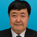 | Development of Digital Type CMOS-MEMS Cointegrated Pressure Sensor Using Cost-Effective Minimal Fab Tools | Yongxun Liu received the B.S. degree in electronics engineering form Jilin University, China, in 1983 and the M.S. and Ph.D. degrees from Tohoku University, Sendai, Japan, in 1996 and 1999. From 1999 to 2001, he was a Research Assistant at the department of Mechatronics and Precision Engineering, Tohoku University, where he worked on MEMS devices. From 2001 he joined the National Institute of Advanced Industrial Science and Technology (AIST), Tsukuba, Japan, where he has been engaged in the research and development of nanoscale silicon devices such as double-gate MOSFETs and silicon quantum dots as well as the MEMS sensors. |
| 2-4: Inorganic Nanomaterials 29B-3-1 13:30, October 29 | Prof. Nobuhiro Matsushita, Tokyo Tech., Japan | NANO-STRUCTURE CONTROLS AND DEVICE APPLICATIONS OF SPIN-SPRAYED CuO AND Cu2O FILMS | Mar. 1990 Dept. of Elect. Eng., Waseda Univ. Nov. 1998 Doctor of Eng. from Tokyo Tech., Doctoral dissertation by submitting the thesis Apr. 1990 Technical Officer, Dept. of Elect. Eng., Faculty of Eng., Tokyo Tech. Oct. 1992 Research Associate, Dept. of Elect. Eng., Faculty of Eng., Tokyo Tech. Apr.1998-Mar.1999 Visiting Researcher, Dept. of Elect. and Comp. Eng., Univ. of Minnesota, USA Apr. 2000 Assistant Professor, Dept. of Physical Electronics, Graduate School of Science and Engineering, Tokyo Tech Mar. 2005 Associate Professor, Materials and Structures Laboratory, Tokyo Tech. Oct.2006-Sept.2008 Scientific Research Senior Specialist, MEXT, Government of JAPAN June. 2015 Associate Professor, Dept. of Mater. Sci. and Chem., Grad. School of Sci. and Eng., Tokyo Tech. Apr. 2018 Professor, Dept. of Mater. Sci. and Eng., School of Mater. and Chem. Tech., Tokyo Tech. Dec. 2019 Senior Advisor to the President, Tokyo Tech. (to present) |
| 2-4: Inorganic Nanomaterials 29B-4-1 15:40, October 29 | Dr. Takuya Masuda, NIMS and Hokkaido Univ., Japan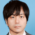 | in situ observation of electrochemical lithiation/delithiation of Si thin film electrodes by X-ray photoelectron spectroscopy | Takuya Masuda obtained his PhD in physical chemistry from Hokkaido University in 2006. He was a postdoc researcher at Arizona State University from 2006 to 2007 and an assistant professor at Hokkaido University from 2007 to 2010. He joined the NIMS in 2010, and is now the group leader of the Battery Materials Analysis Group since 2018 and the deputy director of the Center for Green Research on Energy and Environmental Materials since 2021. He is working on the development of novel in situ techniques for observing energy conversion processes taking place in fuel cells and rechargeable batteries. |
| 2-5: Organic Nanomaterials 29C-4-1 15:30, October 29 | Prof. Yuki Nagao, JAIST, Japan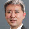 | Highly proton-conductive polymer thin films with organized structure and molecularly oriented structure | Dr. Yuki Nagao is the Associate Professor in the School of Materials Science at Japan Advanced Institute of Science and Technology (JAIST), Japan. He received his Ph.D. in 2006 from Kyushu University. He was appointed as an Assistant Professor of the Department of Mechanical Engineering at Tohoku University in 2006. He also worked as a researcher at PRESTO, JST in 2010, later moving to the Department of Chemistry, Faculty of Science at Kyoto University. From 2012, he works in the present place. His current interest is the research on interfacial ion conduction-based materials and sensors. |
| 2-6: NanoTool 29B-2-1 / Keynote-26 10:10, October 29 | 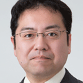 Prof. Yoichiroh Hosokawa, NAIST, Japan | Applications of femtosecond laser amplifier to microprocesses for biological cells | Yoichiroh Hosokawa received the B.S. degree in Applied Physics from Osaka City University in 1995, and M.S. and Ph.D. degrees in Applied Physics from Osaka University in 1997 and 2000, respectively. He has been Joint Associate Professor in the Institute of BioPhotonics, National Yang Ming University, Taiwan, since 2016. His interest is in the investigation of strong photo-excitation phenomena induced by intense ultra-short pulse lasers and their applications to the manipulation and analysis of biological cells and tissues. |
| 2-6: NanoTool 29B-2-2 10:50, October 29 |  | Fabrication and observation of nanopore in two-dimensional materials using Helium ion microscope | Kentaro Kawai received his Dr. Eng. in nano-science and nano-engineering in 2010 from Waseda University, Japan. He was a Research Associate at Waseda University from 2008 to 2010. He is currently an assistant professor at Osaka University, Japan. His research focuses on nano/micro-machining, fluid circuit in microsystem, and biosensing devices. |
| 3: Nanoimprint, Hybrid-NIL, Biomimetics, and Functional Surfaces 29A-5-1 17:30, October 29 | Prof. Akira Saito, Osaka Univ., Japan | Technology Transfer from Reflection to Transmission on the Optical Devices inspired by Morpho Butterfly | Akira Saito is an Associate Professor at Osaka University since 2008. He studied surface physics at the Univ. of Tokyo using Synchrotron Radiation (SR), and received Ph.D. in 1994. He worked at the European SR Facility (Grenoble, France) with French Government Scholarship and at KEK (Japan) to study surface structures with atomic resolution using X-rays. His research interests span the photon-nanomatter interactions, including the analysis, control and fabrication of the surface nanostructures. One of the recent developed fields is bio-mimetic applications of the optical nanostructures in visible-light region, especially based on the Morpho butterfly’s specific optical properties. |
| 4: BioMEMS, Lab on a Chip, and Nanobiotechnolog 28C-3-4 14:30, October 28 | Prof. Takafumi Fukushima, Tohoku Univ., Japan | In-Mold Flexible Hybrid Electronics (FHE) Based on Advanced Wafer-Level Packaging with Chiplets | Takafumi Fukushima received his Ph.D. degree in Department of Materials Science and Chemical Engineering from Yokohama National University in 2003. From 2004 to 2009, he was an assistant professor at the Department of Bioengineering and Robotics, Tohoku University. Since 2010, he has been an associate professor at NICHe, Tohoku University. From 2016 to 2017, He was a visiting faculty at Electrical Engineering Department, UCLA. He is currently working on 3D/heterogeneous integration and Flexible Hybrid Electronics (FHE) technologies at Department of Mechanical Systems Engineering, Tohoku University, as an associate professor. He is a senior member of IEEE. |
| 6: Atomic Layer Processing (ALP) 28B-5-5 20:20, October 28 | Prof. Chang-Yong Nam, Brookhaven National Laboratory, USA | Vapor-phase infiltration for microelectronics applications | Dr. Chang-Yong Nam is a Scientist at the Center for Functional Nanomaterials (CFN) of Brookhaven National Laboratory (BNL) and an Adjunct Professor of Materials Science and Chemical Engineering at Stony Brook University. Dr. Nam joined BNL as a Goldhaber Distinguished Fellow in 2007 and was raised through the ranks to a Scientist in 2016. Dr. Nam received his Ph.D. in Materials Science and Engineering from University of Pennsylvania (2007), M.S. from KAIST (2001), and B.E. from Korea University (1999). His current research is focused on the development of atomic layer deposition (ALD) and associated methods towards microelectronics and energy technology applications. |
| 6: Atomic Layer Processing (ALP) 28B-5-1 18:30, October 29 | Mato Knez, CIC nano, GUNE BRTA, Spain | Atomic Layer Processing: A toolbox for fabricating novel functional hybrid materials | Mato Knez studied chemistry and 2003 finished his doctoral degree in natural sciences at the Max-Planck Institute of Solid-state Research in Stuttgart (Germany). Thereafter he moved to the Max-Planck Institute of Microstructure Physics in Halle, where he led a junior research group. In 2012 he moved to CIC nanoGUNE in San Sebastian (Spain) for an Ikerbasque research professorship and a group leader position where he works until now. Besides his research work he is teaching at the Technical University of Navarra (TECNUN) and scientifically advising and consulting the start-up company CTechnano. His research focuses on thin films and hybrid materials obtained or functionalized by atomic layer deposition (ALD) and related technologies such as molecular layer deposition (MLD) and vapor phase infiltration (VPI). For his research involving ALD he received the Nanofutur award by the German ministry of education and research (BMBF) in 2006 and the Gaede Prize by the German Vacuum Society in 2012. Between 2012 and 2017 he was additionally a Marie-Curie fellow. In 2019 he became honorary professor at the University of Rijeka (Croatia). |
| 6: Atomic Layer Processing (ALP) 28B-5-2 19:00, October 28 | Prof. Woohee Kim, Hanyang Univ., Korea | Process overview of Advanced Area Selective Deposition Methods |


