Keynote Lecture

Key Note Lectures are only available on-demand from Oct 26 with longer lecture time for enough explanation on important topics. No live session will be held. If you have questions or comments about contents in the lecture, please ask questions by chat box.
| Section | Name, Affiliation and Photo | Paper Title | Short Biography |
|---|---|---|---|
| 1-1: Advanced Lithography and Patterning |  Dr. Harry Levinson, HJL Lithography, USA | High NA EUV lithography: Current status and outlook for the future | Harry J. Levinson is currently an independent lithography consultant. He spent most of his career working in the field of lithography. Dr. Levinson has published numerous articles on lithographic science and is the author of three books on lithography. Dr. Levinson is an SPIE Fellow. In recognition of his contributions to SPIE, he received the Society’s 2014 Directors’ Award. Dr. Levinson is currently Editor-in-Chief of the Journal of Micro/Nanopatterning, Materials, and Metrology. He has a PhD in physics from the University of Pennsylvania. For his Ph.D. thesis work, he received the Wayne B. Nottingham Prize in surface science. |
| 1-2: Electron and Ion Beam Technologies | 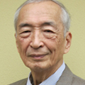 Prof. Masayoshi Esashi, Tohoku Univ., Japan | DEVELOPMENT OF MASSIVE PARALLEL ELECTRON BEAM WRITE (MPEBW) SYSTEM : AIMING AT DIGITAL FABRICATION OF INTEGRATED CIRCUIT | Masayoshi Esashi received the Doctor of Engineering degree in electronic engineering in 1976 at Tohoku University. He served as a research associate from 1976 and an associate professor from 1981 at the Department of Electronic Engineering, Tohoku University. He has been a professor in Department of Precision Engineering since 1990, in The World Premier International Research Center Advanced Institute for Materials Research (WPI-AIMR) since 2007 and in the Micro System Integration Center (μSIC) since 2017 in Tohoku University. He is now CTO in MEMS Core Co. Ltd and concurrently senior research fellow, μSIC in Tohoku University since 2019. He has been studying microsensors, MEMS (Micro Electro Mechanical Systems) and integrated microsystems. |
| 1-3: Patterning Materials |  Dr. Dario L. Goldfarb, IBM Watson Research Center, USA | Evolution of patterning materials towards the Moore's Law 2.0 Era | Dario Goldfarb is a Research Staff Member at the IBM Watson Research Center located in Yorktown Heights, NY (USA). He received his doctorate degree in the field of Physical Chemistry from the University of Buenos Aires, Argentina in 1999 and held visiting scholar and post-doctoral positions at Oxford University (UK) and University of Wisconsin-Madison, (USA). He joined IBM in 2000 and is focused on the understanding of the fundamental properties, limits and applicability of lithographic materials and processes for the patterning of future semiconductor technology nodes. He has authored and co-authored over 80 technical publications and holds over 80 patents. |
| 2-1 Nanocarbon & 2D Materials | 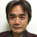 Prof. Kazu Suenaga, Osaka Univ., Japan | Low-dimensional carbon nanostructures: From graphene to carbon atomic chains | Kazu Suenaga got his Ph.D in Materials Science at the University of Tokyo in 1994. He was a postdoctoral fellow at Ecole Nationale Superieure des Mine de Paris (1994–1997) and at the Solid State Physics Laboratory in the University Paris-Sud (1997–1998). Then he joined the Japan Science and Technology Corporation (JST) (1998–2001), National Institute of Advanced Industrial Science and Technology (AIST) (2001-2021) and is now a professor in Osaka University since 2021. A recipient of the Seto award (Japanese Society of Microscopy 2005), winner of the Sir Martin Wood prize (the British Embassy 2006) and grantee par JST-CREST/ACCEL (2006-2011, 2012-2017, 2020-2026) for the "Triple-C" project. His major research theme involves the single atom spectroscopy and the single molecular imaging by means of TEM/STEM. |
| 2-2: Nanodevices | |||
| 2-3: Nanofabrication | 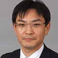 Prof. Futoshi Iwata, Shizuoka Univ., Japan | Development of probe microscope techniques for nanofabrication and manipulation | Futoshi Iwata is a professor in department of mechanical engineering, Shizuoka University. He is also a professor at research institute of electronics at Shizuoka University. After receiving M.E. from Shizuoka University in 1992, he joined Fujitsu Limited (in the semiconductor device process development division). He joined Shizuoka University as an assistant professor in 1994, received Ph.D. in 1998, became an associate professor in 2002. In 2005, he researched at California Institute of Technology (USA) as an overseas research fellowship. He has been a professor at Shizuoka University since 2010. His interest is in the development of nano fabrication and manipulation techniques using microscopes. |
| 2-4: Inorganic Nanomaterials | 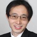 Prof. Mitsuru Takenaka, Univ. of Tokyo, Japan | Materials drive Si photonics | Mitsuru Takenaka received his B.E., M.E., and Ph.D. degrees in electronic engineering from the University of Tokyo, Japan, in 1998, 2000, and 2003, respectively. During 2003-2007, he was a research fellow of the Optoelectronics Industry and Technology Development Association. In 2007, he joined the Department of Electrical Engineering, the University of Tokyo, as a lecturer. In 2008, he became an associate professor. Since 2020, he is a professor at the Department of Electrical Engineering and Information Systems, the University of Tokyo. His research interests presently focus on the heterogeneous integration of III-V/Ge/2D materials on a Si photonics platform. |
| 2-5: Organic Nanomaterials | |||
| 2-6: NanoTool | 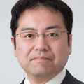 Prof. Yoichiroh Hosokawa, NAIST, Japan | Applications of femtosecond laser amplifier to microprocesses for biological cells | Yoichiroh Hosokawa received the B.S. degree in Applied Physics from Osaka City University in 1995, and M.S. and Ph.D. degrees in Applied Physics from Osaka University in 1997 and 2000, respectively. He has been Joint Associate Professor in the Institute of BioPhotonics, National Yang Ming University, Taiwan, since 2016. His interest is in the investigation of strong photo-excitation phenomena induced by intense ultra-short pulse lasers and their applications to the manipulation and analysis of biological cells and tissues. |
| 3: Nanoimprint, Hybrid-NIL, Biomimetics, and Functional Surfaces | 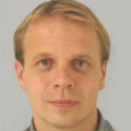 Prof. Jussi Hiltunen, VTT Technical Research Centre of Finland | Roll-to-roll fabrication of lab-on-chip devices | Jussi Hiltunen, Dr. (Tech) joined VTT in 1999 and is currently Research Professor in the “Sensing and Integration” -Research Area. He received doctoral degree from the University of Oulu and has been a visiting researcher at Massachusetts Institute of Technology, University of Southampton and University of California – Berkeley. His research interests are in the roll-to-roll fabrication of microsystem technologies with particular focus on the low-cost environmental and biosensing applications based printed electronics, photonics and microfluidics. He is a board member of Printocent innovation centre advancing the collaboration between the academia and industry on printed electronics and photonics. Jussi-Hiltunen.jpg |
| 4: BioMEMS, Lab on a Chip, and Nanobiotechnolog | 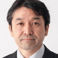 Prof. Takanori Ichiki, Univ. of Tokyo, Japan | Biodevice Technology: From Fundamentals to Applications | Takanori Ichiki obtained his M.S. and Ph.D. degrees in Metallurgy from the University of Tokyo in 1992 and 1995, respectively. He joined the Department of Electric and Electronics Engineering, Toyo University in 1995, where he studied ULSI nano/microfabrication technology and extended it to the nanobiodevice. In 2004, he was assigned to the University of Tokyo, as Associate Professor of the Department of Bioengineering and Institute of Engineering Innovation from 2006 to 2015. In 2016 he was appointed Professor of the Department of Materials Engineering and Department of Bioengineering. He is also the Principal Research Scientist/Laboratory Head of Innovation Center of NanoMedicine (iCONM), Institute of Industry Promotion-Kawasaki, which launched in 2015. His current research activities include the development of point-of-care testing devices, a high-speed enzyme molecule evolution system using in situ synthesized ultrahigh-density microarray chips, and an analytical platform for nanoparticles such as exosomes. |
| 5: Microsystem Technology and MEMS | 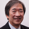 Prof. Isao Shimoyama, Toyama Prefectural Univ., Japan | MEMS Piezo-resistive Strain Gages with Expanding Applications | Isao Shimoyama received the B.E., M.E, and Dr. of Engineering degrees in mechanical engineering from University of Tokyo in 1977, 1979, and 1982, respectively. He joined University of Tokyo in 1982 and served as the Dean of Graduate School of Information Science and Technology from 2007 to 2010. He also served as Director of Information and Robot Technology (IRT) Research Initiative for aging society at University of Tokyo till 2019. He is currently President, Toyama Prefectural University, and Professor Emeritus, University of Tokyo, working with MEMS, MEMS sensors for robots. |
| 6: Atomic Layer Processing (ALP) | 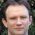 Dr. Christian Dussarrat, Air Liquide, Japan | POWDER ALD: A MATERIALS SUPPLIER’S PERSPECTIVES |


