Symposium A: Emerging Breakthroughs in Materials, Processes and Equipment for Advanced Lithography
(Litho Breakthrough Symposium).
| Section | Name, Affiliation, Paper Title and Short Biography |
|---|---|
| Symposium A: Emerging Breakthroughs in Materials, Processes and Equipment for Advanced Lithography (Litho Breakthrough Symposium)’’. Organizers: Seiji Nagahara (Tokyo Electron), Kouji Asakawa (KIOXIA), Sachiko Kobayashi (Kioxia), Tetsuo Harada (Univ. of Hyogo), Makoto Sakakibara (Hitachi), Hiroshi Yamashita (Nuflare Technol.), Junichi Yanagisawa (Univ. of Shiga Pref.), Tomoki Nagai (JSR) and Julius Santillan (Osaka Univ.) |
|
 | Mr. Toshiyuki Hisamura, AMD, USA Title: Lithography Advancement enabling High‐Performance and Adaptive Computing |
| Toshiyuki (Toshi) Hisamura is Principal Member of Technical Staff at AMD. He has been managing lithography and mask technology development group since he joined Xilinx in 2000 which was acquired by AMD in February, 2022. Prior to that, he held variety of roles involving international business development at Toppan Printing. Hisamura holds two U.S. patents. He earned a bachelor's degree from Waseda University in 1987. |
|
 | Dr. Yoji Watanabe, Nikon, Japan Advanced Lithography and Patterning Application of DUV optical maskless scanner for fabrication of large area device with high resolution |
| Yoji Watanabe is a section manager who is responsible for technology development of Digital Scanner (DUV optical maskless scanner) at Nikon Corporation. He received his PhD in mechanical engineering from Tohoku University in 2007. | |
 | Dr. Martin Burkhardt, IBM, USA Focus effects through pitch and absorber choice for EUV random logic |
| After working on x-ray lithography at MIT, Martin Burkhardt joined Texas Instruments in 1995, where he worked on optical proximity correction and lithography simulations. From 1998 to 2001 he worked on lens aberrations and simulations for early ArF scanners at ASML in Veldhoven, before joining IBM in 2001. He has since worked on automated layout generation, OPC, and resolution enhancement techniques for advanced lithography nodes at both ArF and EUV wavelengths. More recently, he has worked on simulation of alternate absorber materials for EUV. | |
 | Dr. Vicky Philipsen, imec, Belgium The EUV mask exposed |
| Vicky Philipsen received her PhD degree in solid-state physics from the University of Leuven (Belgium) in 2001. At imec she joined the Advanced Patterning department, where her research domain involves the study of mask 3D imaging effects in lithography (from 193nm to EUV and high NA EUV) both by simulations and experiments. She is leading the project on novel EUV mask absorbers at imec. She is team leader of the imaging and reticles team in the imec Advanced Patterning department. She is member of the SPIE ALP conference committee and of the MNE2022 technical program committee. |
|
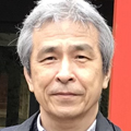 | Prof. Norio Nakamura, High Energy Accelerator Research Organization, Japan High-power EUV free-electron laser for future lithography (tentative title) |
| Norio Nakamura is a professor and leader of the beam dynamics and magnet group in Accelerator Division VI of the Accelerator Laboratory at High Energy Accelerator Research Organization (KEK). His main research subject is advanced light sources such as ERL FELs and next-generation synchrotron radiation sources. He received his Ph. D in Physics from the University of Tokyo in 1987. He worked at the Photon Factory of KEK from 1987 to 1996 and then as an associate professor at the Synchrotron Radiation Laboratory of the Institute for Solid State Physics of the University of Tokyo from 1996 to 2011. | |
 | Mr. Takahiro Ueda, LINTEC OF AMERICA, USA CNT based pellicles for the next generation of EUV scanners |
| Takahiro Ueda joined LINTEC Corporation in 2013 and developed functionalized adhesive tapes. Then, he got transferred to R&D division in LINTEC OF AMERICA, INC to commercialize carbon nanotube materials. Currently, he is working on EUV pellicle development utilizing carbon nanotubes as a team leader. He received his B.S. and M.S. degree in engineering, majoring in optics of soft materials, from Tokyo Institute of Technology in 2011 and 2013, respectively. |
|
 | Dr. Guido Salmaso, ASML, The Netherlands 0.33 NA EUV systems and EUV pellicles for high volume manufacturing |
| Guido has over 15 years’ experience in product development, plasma physics, surface science, thin film coatings, EUV lithography and more. He completed a PhD in Materials Science at Padova University, Italy, in 2005, with a study on EUV multilayers reflective coating. Guido joined ASML in 2014. From 2016 to 2021 Guido worked as product system engineer, leading the development of EUV pellicles to the high volume manufacturing required standards. From 2021 Guido works as senior product system engineer for the 0.33 NA EUV systems platform. | |
 | Dr. Jan van Schoot, ASML, The Netherlands High-NA EUV: getting closer to industry introduction |
| Jan B.P. van Schoot, PhD, Director of System Engineering, ASML, Netherlands. After his study Electrical Engineering (Cum Laude) at Twente University of Technology, he received his PhD in Physics on the subject of non-linear optical waveguide devices and held a post-doc position studying waveguide based electro-optical modulators. He joined ASML in 1996 and held several positions related to Imaging and Optics. In 2007 he joined System Engineering. He was responsible for the Optical Columns of the 0.25NA and 0.33NA EUV systems and the EUV source. He was the study leader of the High-NA EUV system and is now responsible for the High-NA optical train. He is a Sr. Member of the SPIE, holds over 35 patents and presents frequently at conferences about photo lithography. |
|
 | Dr. Gian Lorusso, imec, Belgium High NA EUVL Resist Metrology |
| Gian F. Lorusso received his PhD in solid state physics from the University of Bari, Italy, in 1992. He has been working on topics related to the semiconductor industry such as metrology tool development, lithography, material analysis and more. His domains of expertise include lithography, metrology, microscopy, and spectrometry. After working at the École Polytechnique Fédérale de Lausanne (Switzerland), the Center for X-ray Lithography (Wisconsin), the Center for X-ray Optics at Lawrence Berkeley National Laboratories (California), and KLA-Tencor (California), he has joined IMEC (Belgium) in 2006. His work has produced more than 200 papers and 15 patents. He is working on Extreme Ultraviolet Lithography and Metrology | |
 | Mr. Mohamed Zidan, imec, Belgium Low Landing Energy Electron Beam Metrology of Thin Photoresist using an Aberration-Corrected SEM |
| Mohamed Zidan received his joint master of science in nanotechnology and nanoscience from the universities of KU Leuven and TU Dresden. He is currently a PhD student working on the topic of photoresist metrology for high NA EUV Lithography in the metrology group at imec. | |
 | Dr. Jumpei Yasuda, Mr. Haruyuki Nomura,, Dr. Hiroshi Matsumoto, Mr. Noriaki Nakayamada, and Dr. Hiroshi Yamashita NuFlare Technology, Japan Electron multi-beam mask writer   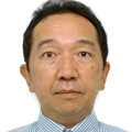  |
| Dr. Jumpei Yasuda received his Ph.D. in physics from Kyushu University, Japan in 2017. He joined NuFlare Technology Inc. in 2017. After joining the company, he worked on the installation of EBM9000 series and then engaged in development work on EBM and MBM series. He is mainly in charge of writing accuracy evaluation, and is currently engaged in the development of new correction functions. Mr. Haruyuki Nomura Haruyuki Nomura received his BS and MS degrees in physics from Tokyo Institute of Technology, Japan in 2011 and 2013, respectively. He joined NuFlare Technology, Inc. in 2013, and is now working on development of electron beam mask writers. Dr. Hiroshi Matsumoto Dr. Hiroshi Matsumoto received his PhD in Earth and Space Science from Osaka University, Japan in 2001. He was a research staff at Japan Atomic Energy Agency (formerly known as Japan Nuclear Cycle Development Institute) from 2001, and at Toyama University from 2004. He joined NuFlare Technology, Inc. in 2007 and is working on development of electron-beam mask writers. Mr. Noriaki Nakayamada Noriaki Nakayamada received his ME degree in nuclear engineering from the University of Tokyo, Japan. He joined Toshiba in 1993 and moved to Toshiba Machine in 1996 to work on the development of the company’s first commercial 50-kV VSB mask writer. For three decades, he has been working on the development of VSB mask writers and multi-beam mask writers. His major achievement was the introduction of correction software for the resist surface charging effect and resist heating effect. Dr. Hiroshi Yamashita Dr. Hiroshi Yamashita received his PhD in Electronic Device Engineering from Kyushu University. He conducted research and development on high-throughput electron-beam direct-write lithography for about 20 years at NEC, UC Berkeley and Selete before joining NuFlare Technology, Inc in 2013. He is currently working on development of next generation electron-beam mask writers |
|
 | Mr. Tomoyasu Shojo, Hitachi, Japan Inspection and metrology challenges for 3 nm node devices and beyond |
| Tomoyasu Shohjoh has joined to Research & Development group, Hitachi, Ltd. from 2005, and has engaged in research of electron optics system for Defect Review SEM and CD-SEM. And he had joined to imec as assignee of Hitachi High-Tech Corporation from 2019, and had worked on the application development of metrology with SEM technology for advanced semiconductor process. He received his B.S. degree in Physics and M.S. degree in Science and Engineering from Tsukuba University, Japan, in 2003 and 2005, respectively. | |
 | Dr. Linyong Pang, D2S, USA Inverse lithography technology: 30 years from concept to practical, full-chip reality |
| Linyong (Leo) Pang received his PhD in mechanical engineering and an additional MS degree in computer science from Stanford University. Currently, he is the Chief Product Officer and Executive Vice President at D2S, Inc. Prior to D2S, he was the GM and Sr. Vice President of Luminescent Technologies. He is most widely known as the person who coined the term, “Inverse Lithography Technology” or “ILT,” and who brought curvilinear ILT into the lithography and photomask world. Prior to joining Luminescent, he held several product development and marketing management positions at Numerical and Synopsys (after acquisition), and was a research scientist at Acuson. He has 38 issued patents, 27 pending patents, and 85 publications. | |
 | Dr.Hamed Sadeghian, Nearfield Instruments B.V., The Netherlands High-Throughput Scanning Probe Microscopy for Semiconductor Metrology and Inspection (Invited) |
| Dr. Hamed Sadeghian Co-Founder, President and CEO of Nearfield Instruments Dr. Sadeghian invented and developed the first high throughput, multi-head AFM system for metrology and inspection of high-end semiconductor manufacturing process control. He also inveted and developed the Sub-Surface AFM, for non-destructive, high resolution imaging of deep buried nano-structures through opaque layers. In 2016, Dr. Sadeghian has co-founded Nearfield Instruments, a semiconductor equipment company, offering highly innovative metrology and inspection solutions for semiconductor manufacturing industry. He is currently CTO/CEO at this scale-up company. Dr. Sadeghian received his PhD (Cum Laude) in 2010 from Delft University of Technology. Four years later he received an MBA degree from the Vlerick Business School in Belgium. He is the founder (2001) of Jahesh Poulad Co., a manufacturer of mechanical equipment, where he sold the company in 2006. Previously, he was scientific director of NOMI (Nano-Optomechatronics Instrumentation) at TNO in The Netherlands from 2011 to 2018 Dr. Sadeghian is a part time associate Professor at the Technical University of Eindhoven. He holds more than 70 patents, and published over 100 peer-reviewed technical papers. |
|
 | Dr. Onoue Takahiro, HOYA Corporation, Japan Development of EUV blanks and future challenges |
| Dr Takahiro Onoue is the Senior Director of the Technology & Development I group in HOYA's LSI division. He received his Ph.D degree in applied chemistry from Waseda University. Majoring in functional thin film deposition. He was a researcher at the University of Twente (The Netherlands). He joined HOYA corporation in a leading position in R&D for magnetic thin film for hard disk drives. In 2011 he joined the LSI division where his main responsibility has been EUV and optical blanks development. | |
 | Mr. Toshiyuki Todoroki, Lasertec, Japan Actinic patterned mask inspection for EUV Lithography |
| Toshiyuki Todoroki graduated from Chiba University in 2008 with a master's degree in applied physics. After graduating, he joined Lasertec Corporation, where he has been designing and developing inspection and measurement algorithms and high-speed processing systems for mask inspection systems, SiC wafer inspection systems, and confocal microscopes. Since 2018 he has been the leader of the group engaged in developing the Die to Database inspection function for the Actinic EUV Patterned Mask Inspection System. |
|
 | Prof. Redouane Borsali, Polynat, France Self-assembly of Carbohydrate Block Copolymers:Sub_10nm Nanostructured Thin films |
| Prof.RedouaneBorsali_ShortBio_MNC | |
 | Prof. Gregory Denbeaux, SUNY, US Controlling EUV resist stochastics |
| Greg Denbeaux received his BA degree in physics from Wesleyan University in 1993. He studied free electron lasers and x-ray microscopy for his PhD from Duke University in 1999. He was a staff scientist at Lawrence Berkeley National Laboratory until becoming faculty at the College of Nanoscale Science and Engineering, Albany, New York. Currently, he is an associate professor at SUNY Polytechnic Institute and studies fundamentals of photoresists including stochastic effects, outgassing, and secondary electron interactions. He also has a research program in nanoparticle detection, quantification, identification and transport, all aimed at defectivity reduction in semiconductor manufacturing. He has published over 200 papers on this research which have been cited over 2,500 times. He has organized the IEUVI Resist Technical Working Group (TWG) for the last few years. | |
 | Prof. Alex P. G. Robinson, Univ. of Birmingham, UK Progress in The Multi Trigger Resist |
| Alex Robinson is co-founder, and Chief Technical Officer of Irresistible Materials Ltd, a Senior Lecturer in the School of Chemical Engineering at the University of Birmingham, and founder and director of Chromatwist Ltd. He has over twenty years of experience of research in materials and processes for nanofabrication, including EUV photoresist development, and ultrahigh spin-on carbon hardmasks. Other research interests include the integration of top-down lithography with bottom-up self-assembly of aptamer biosensing molecules for biodetectors, novel nanostructured catalysts via synthetic biology approaches, and investigations of ultra-high Stokes shift organic fluorescent materials for bio-imaging applications. |
|
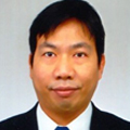 | Prof. Julius Joseph Santillan, Osaka Univ., Japan Realtime analysis of pattern formation during the resist development process |
| Dr. Julius Joseph Santillan has worked on lithographic technology for the last 18 years. He has authored and published numerous papers related to resists and process for various lithographic technologies (F2, ArF immersion, EUV). He received his PhD in engineering from the University of Tsukuba in 2014. Presently, his work is focused on patterning materials / processes and the development of related metrologies at Osaka University. | |
 | Dr. Yanagita Hiroshi, Merck Electronics, Japan Development of rinse materials in advanced lithography and patterning |
| Hiroshi Yanagita has been serving as senior scientist in Global R&D at Merck since 2020 on development of EUV related materials. After joining Merck Electronics in 2011, Yanagita engaged in development of underlayers and photoresist for DUV as a scientist. Prior to Merck Electronics, Yanagita received a Ph.D. degree in organic chemistry at Kyushu University in 2007. Yanagita worked as a post doctor in organic chemistry at North Dakota state University from 2007 to 2009 and at Chiba University from 2009 to 2011 respectively. |
|
 | Dr. Danilo De Simone, IMEC, Belgium EUV Lithography patterning: status and challenges towards High-NA |
| Danilo De Simone holds a MS degree in chemistry from the university of Palermo (Italy) and has 22 years of experience in semiconductor R&D field. He led the development of lithographic materials for 90nm and 65nm memory devices for STMicroelectronics (STM) in Italy and covered the role of assignee at STM Alliance in France and STM in Singapore. In 2008, he joined Numonyx to lead the R&D development for lithographic materials and 32nm double patterning for PCM devices. In 2011, he moved to Micron Technology to introduce 45nm phase-change-memory devices in HVM, and to develop patterning solutions for novel devices. In 2013, he joined the international nanoelectronics research center imec leading the research on patterning materials for EUV lithography. | |
 | Dr. Douglas J. Guerrero, Brewer Science Inc., USA Patterning concepts using ultrathin layers |
| Douglas Guerrero completed a PhD in Organic Chemistry from the University of Oklahoma and Post-doctoral work at the University of Texas-Dallas in the field of conducting polymers. He joined Brewer Science in 1995 where he is a Senior Technologist and has been on assignment at imec in Leuven, Belgium since 2008 where he is developing processes for future nodes. Dr. Guerrero is a Senior Member of SPIE and current chair of the SPIE Advances in Patterning Materials and Processes conference. He has published over 60 papers and patents on optoelectronic materials, reflection control, underlayers for EUV lithography, and DSA. |
|
 | Mr. Toru Fujimori, FUJIFILM Corporation, Japan Recent progress of EUV resist development for improving Chemical stochastic |
| TORU FUJIMORI, is a Senior Expert. He joined FUJIFILM Corporation in 1991. He has been studying for synthesizing materials for photo films for 3 years, and then for photo resists for 8 years. In 2002, He’s moved to electronic materials research laboratories to study color resist for image sensor. Since 2008, he has been studying photo resist materials for KrF, ArF, ArF immersion, EB and EUV lithography as a research manager. From 2014 to 2016, he was senior researcher at EIDEC (EUVL Infrastructure Development Center, Inc.). He has filed over 200 patents, described lots of papers, presentations and text book. |
|
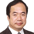 | Dr. Hakaru Mizoguchi, Gigaphoton, Japan Progress of DUV and EUV light source for Lithography, and its new Application for High density Packaging of Semiconductor |
| Prof. Dr. Hakaru Mizoguchi is Senior Fellow of Gigaphoton Inc. and Guest-Professor of Kyushu University. He is Fellow of SPIE since 2019, and member of several academic societies. He joined Komatsu ltd. in 1982 and developed CO2 laser. He was guest scientist of Max-Plank Institute in Goettingen, Germany (1989-1990). He concentrated on Excimer laser for lithography since 1990. Gigaphoton Inc. was founded by his job in 2000. He organized National EUV program (2002-2010), since then he has been promoting EUV light source development. He got Sakurai award from OITDA Japan in 2018. He got IAAM Scientist Award in 2020. |
|
| Panel Discussion on Emerging Breakthroughs in Materials, Processes and Equipment for Advanced Lithography Facilitator: Seiji Nagahara (TEL) and Koji Asakawa (KOXIA) Panel Discussion Opening: Seiji Nagahara, TEL, Japan Position Talks from Panelists: Toshiyuki Hisamura, AMD, USA: Request from device company on lithography materials, processes, and equipment Jan van Schoot, ASML, The Netherlands: EUV exposure tool related breakthroughs in the past and in the future Toru Fujimori, FUJIFILM Corporation, Japan: EUV materials related breakthroughs in the past and in the future Douglas Guerrero, Brewer Science, USA; Lithography related materials breakthroughs Gian Lorusso, imec, Belgium: Metrology/process related breakthroughs Linyong Pang, D2S, USA: Computational lithography breakthroughs Wrap up:Tetsuo Harada, Univ. of Hyogo, Japan Organizers: Seiji Nagahara (Tokyo Electron), Koji Asakawa (KIOXIA), Sachiko Kobayashi (Kioxia), Tetsuo Harada (Univ. of Hyogo), Makoto Sakakibara (Hitachi), Hiroshi Yamashita (Nuflare Technol.), Junichi Yanagisawa (Univ. of Shiga Pref.), Tomoki Nagai (JSR) and Julius Santillan (Osaka Univ.) |
|
