Key Note Lectures are only available on-demand from Nov. 8 with longer lecture time on important topics.
| Section Name and Affiliation |
|
|---|---|
| 1-1: Advanced Lithography and Patterning | |
 | Prof. Jinho Ahn, Hanyang University, Korea PAPER TITLE Masks and Pellicles for HVM EUV Lithography |
| SHORT BIOGRAPHY Jinho Ahn received his B.S. and M.S. degrees from Seoul National University, and Ph.D. degree from the University of Texas at Austin all in Materials Science and Engineering. He worked for Microelectronics Research Laboratory at NEC, Japan, and joined Hanyang University in 1995 as a professor of Materials Science and Engineering. He worked as a Director of Nano and Convergence Technology at National Research Foundation of Korea, and the Vice President of Academic Research and the President of Industry-University Cooperation Foundation at Hanyang University. He is now the President of Korea Nanotechnology Research Society and the Director of EUV Industry-University Collaboration Center. He received the Semiconductor Technology Lifetime Achievement Award in 2015 from the President of Korea. |
|
| 1-2: Electron and Ion Beam Technologies | |
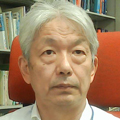 | Prof. Yasuyuki Miyamoto, Tokyo Inst. of Technol., Japan Prof. Nobuhiko Nishiyama, Tokyo Inst. of Technol., Japan Prof. Safumi Suzuki, Tokyo Inst. of Technol., Japan   PAPER TITLE Electron beam lithography in processes for electron/opto/teraherz devices |
| SHORT BIOGRAPHY Yasuyuki Miyamoto is a Professor of Department of Electrical and Electronic Engineering, School of Engineering, Tokyo Institute Technology. He received B.E., M. E., and D.E. degrees in Physical Electronics from Tokyo Institute Technology in 1983, 1985, and 1988, respectively. In 1988 he jointed Department of Physical Electronics, Tokyo Institute of Technology as a Research Associate. He is interested in compound semiconductor electron devices and nano-fabrication process for electron devices. Also, he is in charge of MEXT program ARIM in Tokyo Institute Technology. He is a fellow of JSAP. |
|
| 1-3: Patterning Materials |
|
 | Dr. Peter De Bisschop, Imec, Belgium PAPER TITLE Stochastic effects in lithography: the ultimate resolution limit? |
| SHORT BIOGRAPHY Peter De Bisschop received his PhD in physics from Leuven University, Belgium. He moved to imec in 1986, where he joined the lithography group in 1995. He worked on diverse topics related to exposure-tool-control and -qualification, imaging, masks, rigorous simulations, OPC, and DTCO. His focus in the past few years has been on stochastic effects in EUV |
|
| 2-1: Nanocarbons & 2D Materials | |
 | Prof. Tomoki Machida, Univ. of Tokyo, Japan PAPER TITLE Quantum transport and robotic assembly of van der Waals junctions of 2D materials |
| SHORT BIOGRAPHY Tomoki Machida is a professor at Institute of Industrial Science, University of Tokyo. He received B. Eng., M. Eng., and Ph. D. degrees from University of Tokyo in 1992, 1994, and 1998, respectively. His research interests include quantum transport in van der Waals junctions of graphene and various two-dimensional materials. | |
| 2-2: Nanodevices | |
 | Prof. Satoshi Iwamoto, Univ. of Tokyo, Japan PAPER TITLE Semiconductor-based topological nanophotonics: fundamentals and recent progress |
| SHORT BIOGRAPHY Iwamoto is a professor at the Research Center of Advanced Science and Technology and the Institute of Industrial Science at the University of Tokyo. His research interests include topological photonics and phononics, singular optics, light-matter interaction in photonic nanostructures, and fabrication technology of photonic nanostructures. He received Young Scientist Award of Japanese Society of Applied Physics (2000), the Young Scientists’ Prize, the Commendation for Science and Technology by MEXT, Japan (2012), and the 45th Laser Society of Japan/Distinguished Paper Award (Review Paper Section) (2021). He is a Fellow of Optica (Formerly OSA). |
|
| 2-4: Inorganic Nanomaterials | |
 | Prof. Hitoshi Tabata, Univ. of Tokyo, Japan PAPER TITLE Functional Oxides as a Treasure Box of Oxide Electronics |
| SHORT BIOGRAPHY TABATA graduated from Kyoto University in 1988. He worked at Technical Institute of Kawasaki Heavy Industries from 1988 to 1994 and moved to Osaka University, The Institute of Scientific and Industrial Research as a Research Associate. He was a professor of Nano-science and Nano-technology Center at Osaka University from 2002 to 2006. After 2006, He is currently professor at The University of Tokyo and a fellow of Japan Society of Applied Physics (JSAP). He received a Japan Society for the Promotion of Science (JSPS) Prize in 2008 and outstanding paper award of JSAP in 2013. And he is JSAP fellow from 2014. |
|
| 2-6: NanoTool | |
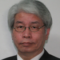 | Prof. Hiroki Kurata, Kyoto University, Japan PAPER TITLE Electronic state analysis with high spatial resolution using STEM-EELS |
| SHORT BIOGRAPHY Kurata is a Professor of the Institute for Chemical Research, Kyoto University. He received D.S. degree in Chemistry from Kyoto University in 1988. He worked at the Institute for Chemical Research, Kyoto University from 1986 to 1996, and moved to the Japan Atomic Energy Research Institute. He was an Associate Professor of the Institute for Chemical Research, Kyoto University from 2002 to 2012. He has been in the current Professor since 2012. His research interests are structural analysis and local electronic structural analysis using scanning transmission electron microscopy combined with electron energy-loss spectroscopy. He received the Japanese Society of Microscopy Award in 2003. |
|
| 4: BioMEMS, Lab on a Chip, and Nanobiotechnology | |
 | Prof. Keiko Tawa, Kwansei Gakuin Univ., Japan PAPER TITLE Application of plasmon-enhanced field to bio-detection with a plasmonic chip |
| SHORT BIOGRAPHY Keiko TAWA is a Professor of School of Biological and Environmental Sciences, Kwansei Gakuin University. She received Doctorate degree from Kyoto University in 1995 and worked as a researcher at Osaka National Research Institute which is reorganized to AIST. After she has worked there and moved to current place in 2015. From 2000 to 2002, she studied at the Max Planck Institute for Polymer Research in Germany on a Humboldt Foundation Research Scholarship. Her research interests are nanobiosensing and imaging with the plasmonic chip which has wavelength-sized periodic structure covered with metal layers by fluorescence microscopy and spectroscopy. |
|
| 6: Atomic Layer Processing (ALP) | |
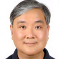 | Prof. Jiyoung Kim, University of Texas PAPER TITLE Atomic Layer Deposition Application for EUV Photo Resist |
 | Prof. Jin-Seong Park, Hanyang University PAPER TITLE Recent Progress of Molecular Layer-Deposited Inhibitor Using Metalcone film for Nanoscale Area-Selective Deposition |
