Symposium A
Symposium A: The Path to Sustainable Lithography.
Symposium A: The Path to Sustainable Lithography. |
|
| _Tomoki Nagai (JSR), Koji Asakawa (Kioxia), Tetsuo Harada (Univ. of Hyogo), Sachiko Kobayashi (Kioxia), Keiichiro Hitomi (Hitachi), Makoto Sakakibara (Hitachi), Junichi Yanagisawa (Univ. of Shiga Pref.), Toru Fujimori (FUJIFILM) and Julius Santillan (Osaka Univ.) | |
Special Talk |
|
Dr. Martin van den Brink, Former President, and CTO, ASML, The Netherlands 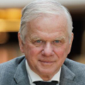 Paper Title AI progression enabled with System Energy Efficient Performance improvements, supported by holistic lithography Short Biography Martin joined ASML in 1984 as an engineer and became Vice President Technology (CTO) in 1995. In 2013, he was appointed Chief Technology Officer and President. Martin earned a degree in electrical engineering from HTS Arnhem (HAN University) and a degree in physics from the University of Twente in the Netherlands in 1984. - Honorary doctorates in mechanics from the university in Eindhoven (2024) - Imec Lifetime of Innovation Award (2019) - IEEE Robert N Noyce Medal for exceptional contributions to the microelectronics industry (2015) - IEEE Cledo Brunetti Award for contributions to nanotechnology (2014) - Knight of the Order of the Dutch Lion (Orde van de Nederlandse Leeuw, 2014) - Honorary doctorate in physics from the University of Amsterdam (2012) - SPIE Frits Zernike Award for Microlithography for outstanding accomplishments in the development of semiconductor lithographic imaging solutions (2008) |
|
Symposium Invited |
|
Prof. Norio Nakamura, High Energy Accelerator Research Organization(KEK), Japan 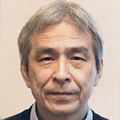 Paper Title EUV-FEL light source for sustainable lithography Short Biography Norio Nakamura is a professor emeritus and researcher at High Energy Accelerator Research Organization (KEK), where he was a professor and leader of the beam dynamics and magnet group in the Accelerator Laboratory from 2011 to 2023. His main research interest is accelerator-based advanced light sources such as high-power free-electron lasers based on energy-recovery linac and next-generation synchrotron radiation sources. He received his Ph. D in Physics from the University of Tokyo in 1987. He worked for the Photon Factory at KEK and then worked as an associate professor in the Institute for Solid State Physics at the University of Tokyo from 1996 to 2011. |
|
Dr. Noriyuki Uchida, AIST, Japan 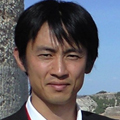 Paper Title Systematic construction of Green and Sustainable semiconductor manufacturing technologies, and the Scope 3 impact of GHG protocol Short Biography Noriyuki UCHIDA received the Ph.D. degree in material science from The University of Tokyo in 2003. He is currently a Director of Research Planning Office of Department of Electronics and Manufacturing at National Institute of Advanced Industrial Science and Technology (AIST), Tsukuba, Japan. He specializes in the study of semiconductor device materials and greener semiconductor manufacturing process. |
|
Dr. Gian Lorusso, imec, Belgium」  Paper Title The Role of Models and Metrology in the Quest for More Sustainable Semiconductor Manufacturing Short Biography Gian F. Lorusso received his PhD in solid state physics from the University of Bari, Italy, in 1992. He has been working on topics related to the semiconductor industry such as metrology tool development, lithography, material analysis and more. His domains of expertise include lithography, metrology, microscopy, and spectroscopy. After working at the École Polytechnique Fédérale de Lausanne (Switzerland), the Center for X-ray Lithography (Wisconsin), the Center for X-ray Optics at Lawrence Berkeley National Laboratories (California), and KLA-Tencor (California), he has joined IMEC (Belgium) in 2006. His work has produced more than 240 papers and 17 patents and was awarded with both the Vladimir Ukraintsev and Diana Nyyssonen awards. He is working on Extreme Ultraviolet Lithography and Metrology, fields in which he started in the early nineties. |
|
Dr. Daniel P. Sanders, IBM Research – Almaden, USA  Paper Title Accelerated Discovery for a Sustainable Semiconductor Short Biography Daniel P. Sanders, Ph.D. is a Principal Research Scientist and Senior Manager in charge of the Materials Discovery department at IBM Research – Almaden. Dan received his Ph.D. in Chemistry from the California Institute of Technology (Pasadena, CA) working in the lab of Prof. Robert H. Grubbs on metal-catalyzed fluoropolymers for 157nm lithography. Dan currently oversees the Materials Discovery department within the Accelerated Discovery organization of IBM Research, whose mission is to develop and apply informatics, simulation, artificial intelligence, and advanced lab automation technologies to speed the discovery of new sustainable materials and apply these tools to pertinent use cases including semiconductors and energy storage. |
|
Mr. Kazuyuki Usuki, FUJIFILM Corporation, Japan 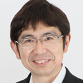 Paper Title Development of UV-NIL resist for semiconductor device manufacturing Short Biography Kazuyuki Usuki joined FUJIFILM Corporation in 1991 after completing his master's degree in engineering at Tohoku University, where he has been involved in research of nanoimprint technology for magnetic recording media since 2006 and in charge of development of nanoimprint materials for semiconductor manufacturing since 2010. More recently, as a senior manager, he has overseen the company's front-end materials development, including EUV resists. |
|
Dr. Arame Thiam, Tokyo Electron Europe, UK  Paper Title EUV Patterning of 2nm node Place’n’Route (PnR) Metal towards High NA: Process Enhancement and Directional Etch using TEL AcreviaTM Gas Cluster Beam (GCB) Technology Short Biography Dr Arame Thiam received her M.Sc. and PhD in Microelectronics and Nanotechnologies from the University of Lille 1 (France). After starting her career in CEA-Leti Grenoble (France) Patterning group working on e-beam lithography, she joined Imec (Belgium) in 2015. Her focus was lithography process development support of Imec Interconnects, Beyond CMOS, OIO and Quantum computing programs. Since 2022, she works at Tokyo Electron Europe supporting High NA EUV lithography joint-development work with imec, focusing on patterning exploration. |
|
Mr. Kimio Ito, DNP, Japan 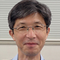 Paper Title Sustainable Semiconductor Lithography through Nanoimprint Technology Short Biography Kimio Itoh joined Dai Nippon Printing in 1996 after completing his master's degree in the Department of Science and Engineering at Keio University. In his first 5 years with the company, he focused on the development of decorative printed materials using EB technology and gained experience with 7ft-wide printing. Since the initiation of the nanoimprint project, he has been actively involved in the development and application of templates. Currently, his primary focus is on template development, particularly for semiconductor lithography, utilizing Multi-Beam Mask Writer technology. |
|
Prof. Toshiyuki Taniuchi, The University of Tokyo., Japan 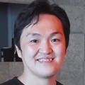 Paper Title Device and Material Characterization by Laser-Based Photoemission Electron Microscopy Short Biography Toshiyuki Taniuchi is a Project Associate Professor at the University of Tokyo. Earning his PhD from the School of Engineering at the university, he specialized in studying magnetic materials by photoemission electron microscopy (PEEM) with synchrotron X-rays. His postdoctoral work at the Institute for Solid State Physics was dedicated to developing ultrahigh-resolution PEEM using lasers. Currently, in his role within the social cooperation research department, he focuses on nanomaterial imaging with laser-based PEEM, in collaboration with the Hitachi Group. |
|
Mr. Kenji Suzuki, Samsung Japan., Japan 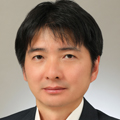 Paper Title Precise non-contact measurement of p-n junction depth using terahertz emission spectroscopy Short Biography Kenji Suzuki received his B.S. degree and M.S. degree from The Tokyo University, Japan in 1999 and 2001, respectively. He joined Research & Development group, Hitachi, Ltd. in 2001 and engaged in development of hard disk drives. From 2021, he has worked on the development of metrology and inspection for semiconductor in Samsung R&D Institute Japan and Samsung Japan Corporation. |
|
Prof. Tsumoru Shintake, OIST, Japan  Paper Title A simple, low-cost, highly energy-efficient, two-mirror projector for EUV lithography Short Biography Prof. Tsumoru Shintake joined OIST in 2011, came back from Stanford University CA, where he was a professor in physics, but for a short period, right after completion as technical leader of SACLA X-ray laser project of RIKEN, in June 2011. I am a beginner in semiconductor lithography, first attend BUCUS 2022. Deeply digging optics from Newton's telescope to today's EUV, I found how to make exposure field wide enough on two-mirror projector, hint from 1840s Petzval theory for flat field. I am enjoying optics now, and I wish I can contribute more in this field. |
|
Dr. Cheng Wang, Lawrence Berkeley National Laboratory, USA 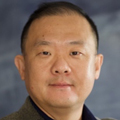 Paper Title Characterization of latent image via critical-dimension resonant soft X-ray scattering Short Biography Dr. Cheng Wang is a Physicist Staff Scientist at the Advanced Light Source, Lawrence Berkeley National Lab. He is currently a PI and thrust lead for multimodal characterization at the Center for High Precision Patterning Science (CHiPPS). He obtained his bachelor’s degree in physics from Jilin University, China in 2002, and received his Ph.D. in physics in North Caroline State University in 2008. After graduation, he joined the ALS, LBNL where he led the development of Resonant Soft X-ray Scattering for soft materials and the construction of a dedicated facility at ALS Beamline 11.0.1.2. His research interest is to develop and utilize advanced synchrotron x-ray probes such as soft x-ray scattering, spectroscopy to elucidate the morphology, chemistry, and interfacial structure of broad range of complex materials |
