MNC 2024 Plenary Speakers List |
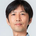
Dr. Yoshihisa Kagawa, Sony Semiconductor Solutions Corporation, Japan
 PAPER TITLE
Novel 3D Stacking Process Technologies to Evolve CMOS Image Sensors |
SHORT BIOGRAPHY
Yoshihisa Kagawa is a general manager of Research Division at Sony Semiconductor Solutions Corporation. He joined Sony Corporation in 2004 and he has been a specialist for BEOL and 3D-stacking process integration. Especially, he contributed to launch Sony’s Cu-Cu hybrid bonding process and announced its rollout at IEDM 2016. Currently, he manages the research and development of process integration for stacked CMOS image sensors. He is a committee member of IEEE Electronic Components and Technology Conference (ECTC) and IEEE International Interconnect Technology Conference (IITC).
SHORT ABSTRACT
In the field of CMOS Image Sensors (CIS), there has been high demand for new functions that can respond various photo taking scenes. We have developed the stacked Back Illuminated-CIS (BI-CIS), composed of conventional BI-CIS technology and standard logic technology. To realize the fine-pitch and large-scale electrical connection between upper CIS chip and lower logic chip, we have developed the wafer-to-wafer Cu-Cu hybrid bonding technology and successfully introduced it to our stacked BI-CIS in 2015. Since then, to fabricate more advanced stacked BI-CISs we have developed various kinds of novel process technologies: 3-wafers stacking process, chip-to-wafer stacking process and ultra-fine pitch Cu-Cu hybrid bonding. In this talk, the process technologies that have evolved the stacked BI-CIS will be discussed. |
Dr. Jan van Schoot, ASML, The Netherlands
 PAPER TITLE
The next step in Moore’s Law: High NA EUV is here |
SHORT BIOGRAPHY
At this moment EUV systems equipped with a 0.33 Numerical Aperture (NA) have proven themselves and are successfully applied in high volume manufacturing. The next step is 0.55 NA and is ready to enter mass production.
This so-called high NA scanner, targeting an ultimate resolution of 8nm, will bring multiple benefits to the semiconductor market such as reduction of process complexity, yield improvement, higher resolution enabling printability of smaller features at increased density, and cost of technology reduction. It will extend Moore’s law for at least another decade.
A novel lens design, capable of providing the required Numerical Aperture, has been identified; this so called anamorphic lens will provide 8nm resolution in all orientations. Paired with new, faster stages and more accurate sensors providing the tight focus and overlay control needed it enables future nodes.
In this talk, I will sketch an overview of the path of more than 12 years development of the High NA EUV scanner. This resulted into a full functional tool, of which the current imaging and overlay performance will be shown. The results are taken from the first tool that resides in the High NA lab.
Jan B.P. van Schoot, PhD, Fellow and Senior Function System Engineer, ASML, Netherlands.
After his study Electrical Engineering (Cum Laude) at Twente University of Technology, he received his PhD in Physics on the subject of non-linear optical waveguide devices and held a post-doc position studying waveguide based electro-optical modulators.
He joined ASML in 1996 and was Project Leader for the Application of the first scanner and its successors up to 5500/750. In 2001 he became Product Development Manager of Imaging Products (DoseMapper, Customized Illumination). In 2007 he joined System Engineering. He was responsible for the Optical Columns of the 0.25NA and 0.33NA EUV systems. After this he worked on the design of the EUV source. He was the study leader of the High-NA EUV system and is now responsible for the High-NA optical train and investigating future extensions.
He is an ASML-Fellow and Fellow of the International Society of Optics and Photonics (SPIE), holds over 55 independent patents and presents frequently at conferences about photo lithography.
|
Dr. Hisashi Saito, Ministry of Economy, Trade and Industry, Japan

PAPER TITLE
Japan’s Semiconductor Strategy |
SHORT BIOGRAPHY
Hisashi Saito is deputy director of IT Industry Division at Ministry of Economy, Trade and Industry (METI). He joined METI in 2021 and he worked on semiconductor R&D budgets and Japan’s semiconductor strategies. Prior to joining METI, he was involved in R&D of GaN and Si power semiconductors and GaN high-frequency semiconductors at a Japanese semiconductor company.
SHORT ABSTRACT
Three years have already passed since the Ministry of Economy, Trade and Industry formulated the “Semiconductor and Digital Industry Strategy” for 2021, and the global situation has changed dramatically. Responding to economic security risks, making the semiconductor supply chain more resilient, and addressing digitalization and greening have become more realistic issues. For this reason, we have just revised our strategy in June last year. This presentation will provide an overview of specific strategies and initiatives, including last year's revision and subsequent updates, mainly related to semiconductors. |
