Invited Speakers

Bulk photovoltaic effect in polar 2D materials
Short Biography
Dr. Eda is Associate Professor of Physics and Chemistry at the National University of Singapore, and a member of the Centre for Advanced 2D Materials (CA2DM). Before joining NUS in 20211, he was a Newton International Fellow of the Royal Society of the UK and worked at Imperial College London. Dr. Eda received his M.Sc. in Materials Science and Engineering from Worcester Polytechnic Institute in 2006 and Ph.D. in the same discipline from Rutgers University in 2009. He is a recipient of the Singapore National Research Foundation (NRF) Research Fellowship and many awards including the Singapore National Academy of Science (SNAS) Young Scientist Award and University Young Researcher Award. He is an Associate Editor of npj 2D Materials and Applications. His research focuses on the electronic, photonic, and magnetic device physics of two-dimensional materials.

Growth Model of CVD-grown Graphene Based on In-Situ Ultraviolet Optical Observation
Short Biography
She received Doctor of Engineering at Kyushu University in 2014. After working as a postdoc at Cornell University, USA, she joined NTT Basic Research Laboratories (NTT-BRL), NTT Corporation, Japan, in 2015. She is now a Senior Research Scientist at NTT-BRL. Her research interests are related to developing growth and understanding growth mechanisms of low-dimensional materials such as graphene.
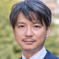
Machanical motion sensing using spintronics devices
Short Biography
He earned his Ph.D. in Engineering from Tohoku University in 2004. Following his doctoral studies, he joined the Japan Science and Technology Agency's Semiconductor Spintronics Project as a Researcher. In 2008, he became an Assistant Professor at Kyoto University and later advanced to Associate Professor in 2012. Additionally, he held academic positions at Osaka University, where he was recognized as an Honorary Professor. In April 2023, he took on the role of Director and Professor at Tohoku University's International Center for Synchrotron Radiation Innovation Smart. His expertise lies in Spintronics.
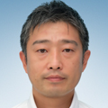
Silicon Integration Technology for Quantum Computing
Short Biography
Takahiro Mori received B.S., M.S., and Ph.D. degrees in applied physics from Tohoku University, Sendai, Japan, in 2001, 2003, and 2006, respectively. He is currently a Leader with the Exploratory Silicon Device Research Team, Semiconductor Frontier Research Center (SFRC), National Institute of Advanced Industrial Science and Technology (AIST), Tsukuba, Japan. He is currently working on the research and development of silicon quantum device integration technology and leading-edge transistors.

Metal chalcogenides on flexible substrates for Robust Electronics
Short Biography
Professor Johnny HO is currently Associate Vice-President (Enterprise), a Professor in the Department of Materials Science and Engineering, a core member in the State Key Laboratory of Terahertz and Millimeter Waves at the City University of Hong Kong (CityU), and a Professor (joint appointment) in Institute for Materials Chemistry and Engineering at the Kyushu University, Japan. He received his BS, MSc, and PhD degrees at the University of California, Berkeley, USA, in 2002, 2005, and 2009, respectively. Due to his outstanding academic performance, Professor Ho was selected for the Intel Foundation PhD Fellowship (2007-2009). Before moving to Hong Kong, he got his postdoctoral training from Lawrence Livermore National Laboratory, California, USA (2009-2010). Professor Ho’s research interests focus on the synthesis, characterization, and applications of nanoscale materials for electronic, optoelectronic, sensor, and energy-harvesting devices.

abrication of n-type and p-type WSe2 field-effect transistors and their low voltage CMOS inverter operation
Short Biography
Takamasa Kawanago is a senior researcher of National Institute of Advanced Industrial Science and Technology (AIST), Tsukuba, Japan. He received Ph.D. from Tokyo Institute of Technology (2011). He is currently working on research and development in device physics and process technology for new materials and structure CMOS transistors.
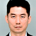
Exploring Two-dimensional-material-based heterostructures
Short Biography
Dr. Ryo Kitaura serves as the group leader of the Two-Dimensional Quantum Materials group at the Research Center for Materials Nanoarchitectonics (MANA), National Institute for Materials Science (NIMS) in Japan. His primary research focus lies in the investigation of the distinctive optical properties exhibited by two-dimensional materials and their heterostructures. His approach encompasses the utilization of thin-film growth techniques, such as metalorganic chemical vapor deposition (MOCVD), to facilitate fabrication, while also engaging in the fabrication of nanodevices and employing advanced spectroscopy for thorough characterizations.
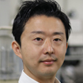
Fast charge transfer via dielectric nano-island
Short Biography
Takashi Teranishi is an Associate Professor in the Division of Applied Chemistry of Okayama University, Japan. He received B. Eng., M. Eng., and Ph. D. degrees in 2004, 2006, and 2010, respectively from Tokyo Institute of Technology. His current research interests include functional materials for lithium ion batteries and microwave/high power characteristics of ferroelectric materials.

Control of Ion Transport in Organized Polymer Thin Films
Short Biography
Yuya Ishizaki received his Ph.D. in 2021 from Tohoku University. From 2021 to 2022 he was a postdoctoral researcher in Tohoku University (Mitsuishi group). He currently joined Nagano group at Rikkyo University from 2022 as an Assistant Professor. His current research interests focus on polymer liquid crystals, fluidic ionic diodes, and neuromorphic materials.
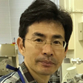
Nanoscale observation of materials and biological samples in liquid by scanning electron assisted dielectric microscopy
Short Biography
Toshihiko Ogura is a chief senior researcher of National Institute of Advanced Industrial Science and Technology (AIST), Tsukuba, Japan. He holds Ph.D. from Toyohashi University of Technology (1997). His research focuses on the development of nanobiotechnology techniques for the direct observation of biological samples and organic materials in solution.

Lifetime prediction of nanoimprint molds
Short Biography
Dr. Jun Taniguchi is a professor in the Department of Applied Electronics at Tokyo University of Science (Tokyo, Japan). He received the BE, ME and PhD degrees from Tokyo University of Science, in 1994, 1996 and 1999, respectively. From 1999 to 2024, he was with Department of Applied Electronics, Tokyo University of Science. His study fields are nanoimprint technology, electron beam lithography and nano-scale fabrication.
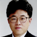
Fish-Mimicking Self-Healing (Super)hyrophilic Films Showing Multifunctional Properties
Short Biography
Atsushi Hozumi is a senior principal scientist of National Institute of Advanced Industrial Science and Technology (AIST), Nagoya, Japan. He holds Ph.D. from Nagoya University (1997). His research focuses on biomimetics and related materials, the control of surface wettability using monolayers, polymer brushes, hybrid films, gels, and their practical applications. Currently, he is the chair of the steering committee of the Research Group on Biomimetics, The Society of Polymer Science, Japan, a visiting professor at Aichi Institute of Technology and a member of the editorial boards of Materials Letters, Elsevier.
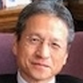
Bio and device meet at Nano
Short Biography
Ichiro Yamashita graduated from Kyoto University and received a Ph.D. degree from the Graduate School of Science, Nagoya University in1998. 1978-2013, he worked at Panasonic Corporation, 2003-2017 at Nara Institute of Science and Technology, and 2013-present at Osaka University. 2014-present, a visiting professor National Yang Ming Chiao Tung University.
His research interests include Nanotechnology, Biomineralization, Aptamer, and Biosensors. He proposed a biological inorganic nanostructure fabrication process, “Bio Nano Process”, in 1997. He discovered anomalous charge-transfer enhancement effects in electrochemistry in 2020 and is developing a DNA sensor based on this discovery. Awards and honors include Human Frontier Science Program. He is a fellow of the Japan Society of Applied Physics.
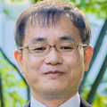
Advancing Polymer MEMS with 3D Photolithography
Short Biography
He received his B.E. and M.E. degrees from Gunma University, Japan, in 1998 and 2000, and his Ph.D. from Kyoto University in 2003. From 2008 to 2015, he was an associate professor at Kagawa University. From 2015 to 2018, he was an associate professor at Gunma University. Since 2018, he has been a professor at the Division of Mechanical Science & Technology, Gunma University. From 2015 to 2019, he was also a PRESTO researcher at JST. His research focuses on microfabrication technology, microfluidic systems for bio applications, and energy harvesting and sensors for IoT.

Understanding of oxidant gas effect on crystal structure and ferroelectricity of atomic layer deposited HfxZr1−xO2 thin films using synchrotron X-ray analysis
Short Biography
Dr. Onaya received his Ph.D. degree from Meiji University, Japan, in 2021. From 2019 to 2020, he was a visiting researcher at the University of Texas at Dallas, USA. From 2021 to 2022, he was a Japan Society for the Promotion of Science Research Fellow PD at National Institute of Advanced Industrial Science and Technology, Japan. Since 2022, he has been an assistant professor at the University of Tokyo, Japan and a visiting researcher at National Institute for Materials Science.
His research interests are atomic layer deposition techniques for ferroelectric HfO2-based films and high-k dielectric films for future semiconductor devices.

Recent Progress on Atomic Layer Deposited Oxide Semiconductor Channel Layers for Emerging Memory Application
Short Biography
Professor Jin-Seong Park is a faculty member in the Division of Material Science and Engineering and the Division of Nano-scale Semiconductor Engineering at Hanyang University. His research focuses on semiconductor materials and devices using Atomic Layer Processes (ALP), including work on oxide semiconductors, gate insulators, and area selective deposition and atomic layer etching techniques. Professor Park completed his Ph.D. at KAIST in 2002 and conducted postdoctoral research at Harvard University from 2003 to 2005. He has published over 280 SCI(E) papers and holds more than 90 patents in active-matrix devices and ALD materials/Processes.
