 |
 |
MNC 2009, November 16-19, 2009
22nd International Microprocesses and Nanotechnology Conference
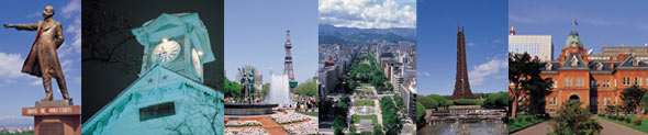
Conference Site: Sheraton Sapporo Hotel, Sapporo, Japan
|

Sheraton Sapporo, Sapporo, Japan |
 |
|
|
 |

MNC 2009 SCOPE and SYMPOSIUM
1-1:DUV, EUV Lithography and Metrology
This session focuses on DUV, EUV, Immersion Lithography, and Computational
Lithography including OPC, SMO, DFM. In addition, Metrology such as SEM
and Scatterometry is included.
1-2:Electron- and Ion-Beam
Lithography
Electron and ion beam technologies such as lithography, metrology, inspection
and repair tools. Other related technologies using charged particle beams
are also welcome.
1-3:Resist Materials and
Processing
Resist materials(EUV, immersion, double patterning, DUV, EB, X-ray, multilayer, inorganic, molecular glass etc.), antireflective coatings, polyimide, adhesive, and other materials related to lithography. resist processes(PEB,development, rinse,resist removal, etching etc.)characterization, line edge roughness, trade-off problem, outgassing, modeling and simulation of resist process (exposure, acid diffusion, development etc.). materials and processes for the production of flat-panel display, photonics devices, and electronics packaging.
2-1:Nanodevices
Nanodevices and related technologies targeting more Moore, more than Moore
and beyond CMOS; next-generation Si and compound semi conductor-based FETs,
graphene FETs, 1D FETs such as nanowire FETs and carbon nanotube FETs,
quantum dot devices, and all other nanodevices utilizing nanostructures
and nanomaterials such as inorganics, organics, and molecules. Novel-concept
devices utilizing nanostructures and nanophysics are also welcome.
2-2:Nanofabrication
Fabrication of nanostructures. Fabrication techniques such as scanning probe techniques, self-organizing techniques, etc. Physics and chemistry in nanofabrication processes. Etching, deposition, and related subsurface processing using photon, electron- and ion-beams, plasma, and thermal energy. Emerging technologies are also welcome.
2-3:Nanomaterials
Theory, properties, characterization and application of nanomaterials
such as quantum dots, nano-particles, nanowires, carbon nanotubes, fullerenes,
organic, molecular, and biomaterials. Materials prepared by self-organized
or bottom-up approach are also included.
2-4:Nano-Tool
Nano-electromechanical system (NEMS), Nano-mechanics, Nanometrology, Metrology
and repair for nanosystem, Novel observation and fabrication methods based
on microscopic techniques, such as scanning probe microscopy (SPM), scanning
electron microscopy (SEM) and focused ion beam (FIB).
3:Nanoimprint,
Nanoprint and Rising Lithography
This session focuses nanoimprint system, process, material, applications
and related inspection and metrology. Other novel nano-patterning technologies
are also included.
4:Bio MEMS, Lab on a Chip
Micro/nano electromechanical devices (M/NEMS) are now widely applied to
biochemical, medical and environmental fields and a new research field
called μ-TAS or Lab. on a Chip is expanding. Fusion of microelectronic
devices with materials and methods in the biomedical fields is expected
to open up new scientific and business areas. Papers are solicited in the
following areas (but not limited): (1) MEMS/NEMS devices for biomedical
fields, (2) μ-TAS and Lab on a chip, (3) Bio-chips for DNA, proteins and
cells, (4) Fabrication technologies.
5:Microsystem
Technology and MEMS
Fabrication techniques, design, mechanical characterization of three dimensional
microstructures, and their applications to micromechanical systems, which
include microwave and photonics devices, vacuum microelectronics, novel
sensors and actuators, etc.
Symposium A. Computational Lithography
Symosium B. Graphene: Growth & Characterization
|
|
|
 |