 |
|
MNC
2016, November 8-11, 2016
29th
International Microprocesses and Nanotechnology
Conference
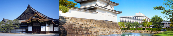
ANA Crowne Plaza Kyoto, Kyoto, Japan |

|
 |
|
|
 |

| ''2D Crystals for Smart Life''
|
 |
|
Abstract
The experimental demonstration of graphene in 2004 has opened up a window
to the two-dimensional (2D) world of materials. This has subsequently triggered
a surge of research activities on various 2D crystals including single
layers of hexagonal-boron nitride (h-BN), several dichalcogenides (such
as MoS2 and WSe2), and complex oxides, with novel electronic properties.
Atomic scale thicknesses (few Å/layer) of 2D semiconducting crystals and
their controllable precise band gaps as a function of number of layers
also enable the scaling of electronic devices without inducing performance
variations. Moreover, seamless planar synthesis and stacking of 2D crystals
on various substrates can be exploited to build novel lateral and vertical
heterostructures, respectively. This talk will highlight and discuss the
prospects of such 2D crystals and their heterostructures for designing
ultra-low power, low-loss, and ultra-energy-efficient active and passive
devices targeted for designing next-generation green electronics needed
to support the emerging paradigm of Internet of Everything. More specifically,
this talk will examine the genesis of the power dissipation challenge in
conventional MOSFETs, and provide an overview of the recently demonstrated
2D-channel tunneling transistor from my group (Nature, 2015) that overcomes
this challenge and is a fundamentally different transistor employing several
innovations. This talk will also bring forward some other applications
uniquely enabled by 2D crystals, including sensors and flexible radio-frequency
electronics for improving quality of life, and discuss related challenges
and opportunities.
|
Short Biography
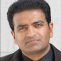
Professor Kaustav Banerjee from UC Santa Barbara is one of the world’s
leading researchers of nanoelectronics. His current research is focused on the
physics, technology and applications of low-dimensional materials such as
graphene and other 2D materials for next-generation green electronics, photonics
and bioelectronics. Initially trained as a physicist, he graduated from UC
Berkeley with a PhD in electrical engineering in 1999.
Professor Banerjee is a Fellow of IEEE and the American Physical Society.
His ideas and innovations have been recognized with numerous awards and honors
including the prestigious Bessel Prize in 2011 from Humboldt Foundation,
Germany, a JSPS Invitation Fellowship in 2013 from the Japan Society for the
Promotion of Science, and the IEEE Kiyo Tomiyasu Award in 2015, one of IEEE's
highest honors.
|
|
|
 |